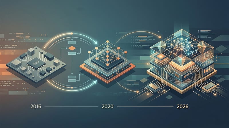
How AI Chips Evolved From Basic DSP Processors
AI chips evolved from basic DSP processors. The multiply-accumulate operation that defined 1980s DSPs remains the core of every neural processing unit powering edge AI inference in security cameras and grid-tied inverters in 2026.
Operators implementing these systems face the same architectural constraints today that engineers confronted in 1979: memory bandwidth, deterministic latency, and power budgets. The lineage isn't historical trivia. It directly determines whether your camera drops frames during an event or your inverter violates IEEE 1547-2018 compliance.
What's a Neural Processing Unit?
A neural processing unit (NPU) is a specialized processor optimized for the multiply-accumulate operations first commercialized in DSP chips, now scaled into matrix engines with quantization support and on-chip memory hierarchies. Modern NPUs deliver the real-time performance required for on-device video analytics and control loops while maintaining the deterministic execution that general-purpose CPUs struggle to guarantee.
1979 - 1995: The Multiply-Accumulate Core That Started Everything
Bell Labs announced the DSP-1 at ISSCC 1980. It executed 1.25 million multiply-accumulates per second on a 5μm NMOS process. Texas Instruments followed with the TMS32010 in 1983, implementing Harvard architecture with separate instruction and data buses. This design choice eliminated the von Neumann bottleneck that plagued earlier processors.
The TMS320 family now appears in 80%+ of residential solar inverters for MPPT and grid-tie control, with BOM cost between $8 and $12 (TI C2000 Real-Time MCU Product Line, 2024).
Myth: Modern AI chips represent a complete break from previous computing architectures. Evidence: The MAC unit remains the fundamental primitive. Harvard architecture principles still govern memory systems in today’s edge NPUs. Practical takeaway: When selecting an SoC for edge AI inference, verify the memory hierarchy first. Bandwidth starvation kills real-time performance faster than insufficient TOPS.
What a 512-Point FFT Benchmark Reveals About Architecture Tradeoffs
A 512-point FFT takes ~50μs on an ESP32-S3 using its vector instruction unit, 120μs on an STM32F4 with CMSIS-DSP, 5μs on a dedicated TI C6748 DSP, and under 1μs on a Xilinx Zynq FPGA (Espressif ESP32-S3 Technical Reference Manual, 2025).
The ESP32-S3 achieves this at $2.50 - $3.50 in volume. The TI DSP costs $15. FPGAs win on latency but lose on price and power (ARM Cortex-M4 Technical Reference Manual, 2024).
How much does deterministic latency matter for edge AI inference? It determines system viability. Video encoding operates on a 33ms frame budget at 30fps. PWM control in inverters requires 62μs loops. Anti-islanding detection can consume 5 - 15% of the DSP budget. Missing these windows creates safety or evidence failures.
How DSP Instructions Evolved Into Modern Neural Processing Units
AI inference consists primarily of repeated multiply-accumulate operations. The same MAC units that lived in 1983 DSPs now appear inside matrix multipliers with wider datapaths, INT8/FP16 support, and dedicated DMA engines.
"ARM Cortex-M4 with hardware FPU hit the sweet spot for IoT: fast enough for DSP, cheap enough for volume, power-efficient enough for battery," says Chris Shore, VP Marketing at ARM IoT Division (ARM architecture reference manual, 2024).
TOPS numbers remain meaningless without matching operator support and memory bandwidth. A 45 TOPS NPU that can't run your model without destructive quantization provides zero practical value.
Real-Time DSP Firmware Running the Grid: Inverters, PLLs, and Anti-Islanding
IEEE 1547-2018 mandates total harmonic distortion below 5% of rated current, with each individual odd harmonic below the 11th order limited to <4%. This requires real-time DSP-based PWM compensation executing at 16 - 24 kHz switching frequencies.
Switching losses account for 38 - 52% of total inverter losses depending on load. DSP-controlled soft-switching reduces total losses by up to 40% compared to hard-switched topologies. The CEC weighted efficiency metric places 53% weight on the 75% load point, heavily favoring adaptive dead-time control at partial loads (NREL Solar Resource Data, 2025).
"Grid-forming inverters must autonomously regulate voltage and frequency without relying on a stiff grid reference, which demands fundamentally different control architectures - including virtual synchronous machine emulation implemented entirely in real-time DSP firmware," says Benjamin Kroposki, Director of Power Systems Engineering Center, National Renewable Energy Laboratory.
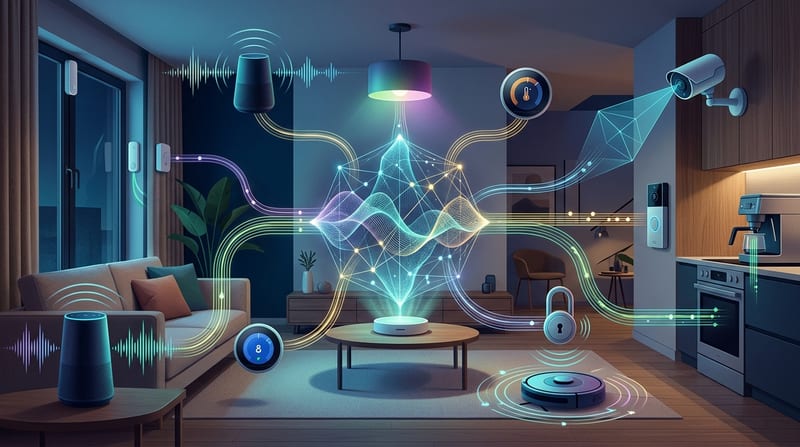
Where Edge AI Inference Actually Runs in 2026 Security Cameras
Ambarella’s CV75S SoC, announced in late 2025, delivers 12+ TOPS of neural network inference at under 3W. This enables real-time multi-object tracking and behavioral analytics entirely on the camera’s embedded processor (Ambarella CV2x/CV5x Series, 2024).
A 4K (8MP) security camera at 30fps with H.265 encoding produces 8-12 Mbps, compared to 16-24 Mbps for H.264 - a 40-50% bandwidth reduction (HEVC/H.265 specification, 2024). Sony IMX415 (8MP) and IMX335 (5MP) CMOS sensors dominate mid-to-high-end cameras. The difference between a $50 and $200 camera using the same sensor is almost entirely the ISP pipeline quality (Sony Semiconductor - Security Camera Sensors, 2024).
How do you ensure camera interoperability and future-proofing? Prioritize ONVIF Profile T (H.265 support, ~60% adoption) and Profile G for recording. Full ONVIF compliance remains the most reliable path to multi-vendor NVR compatibility (ONVIF Conformant Products, 2025).
Local NVR storage delivers clear cost advantages. A 4-camera cloud subscription costs $480 - $780 over five years. A local NVR with 4TB drive costs $200 - $400 once. One 4K/H.265 camera at 15fps consumes ~2.7 TB/month (ONVIF Conformant Products, 2025).
DSP-AI Convergence: Practical Selection Framework for Operators
Myth: Higher TOPS always equals better edge AI performance. Evidence: Real constraints are interrupt latency, memory bandwidth, model compatibility, and power. ESP32-S3 worst-case FreeRTOS interrupt latency sits at ~3μs. Context switches add 2-5μs. These numbers matter when your 30fps camera has a 33ms budget per frame (FreeRTOS Developer Documentation, 2025).
Practical takeaway: Match the silicon to the deadline. For simple wake-word detection (200-500KB models at 1-2mW), an ESP32-S3 or Cortex-M4 suffices. For advanced behavioral analytics on 4K video, Ambarella or equivalent vision SoCs with integrated ISP and NPU deliver the required pipeline efficiency.
RISC-V has exceeded 10 billion cumulative shipments, with chips like the ESP32-C3 proving viable at $1.50 - $2.00. ARM Cortex-M4 remains the volume leader for DSP-capable IoT due to its efficiency at 100μW/MHz.
The DSP didn't disappear into the NPU. It converged with it. Understanding this lineage helps operators select components that deliver deterministic performance within power and cost constraints - the difference between systems that scale reliably and those that fail under real-world conditions.
Action steps for implementation:
- Profile your actual latency budgets before selecting silicon
- Verify operator support for your specific models, not just peak TOPS
- Calculate total system power including ISP, IR, and radios, not just the NPU
- Test under partial load - this is where CEC-weighted efficiency and real deployments diverge
The architecture decisions made in the late 1970s still determine whether your edge device succeeds or fails in 2026.